Semiconductor Lab
Back to overview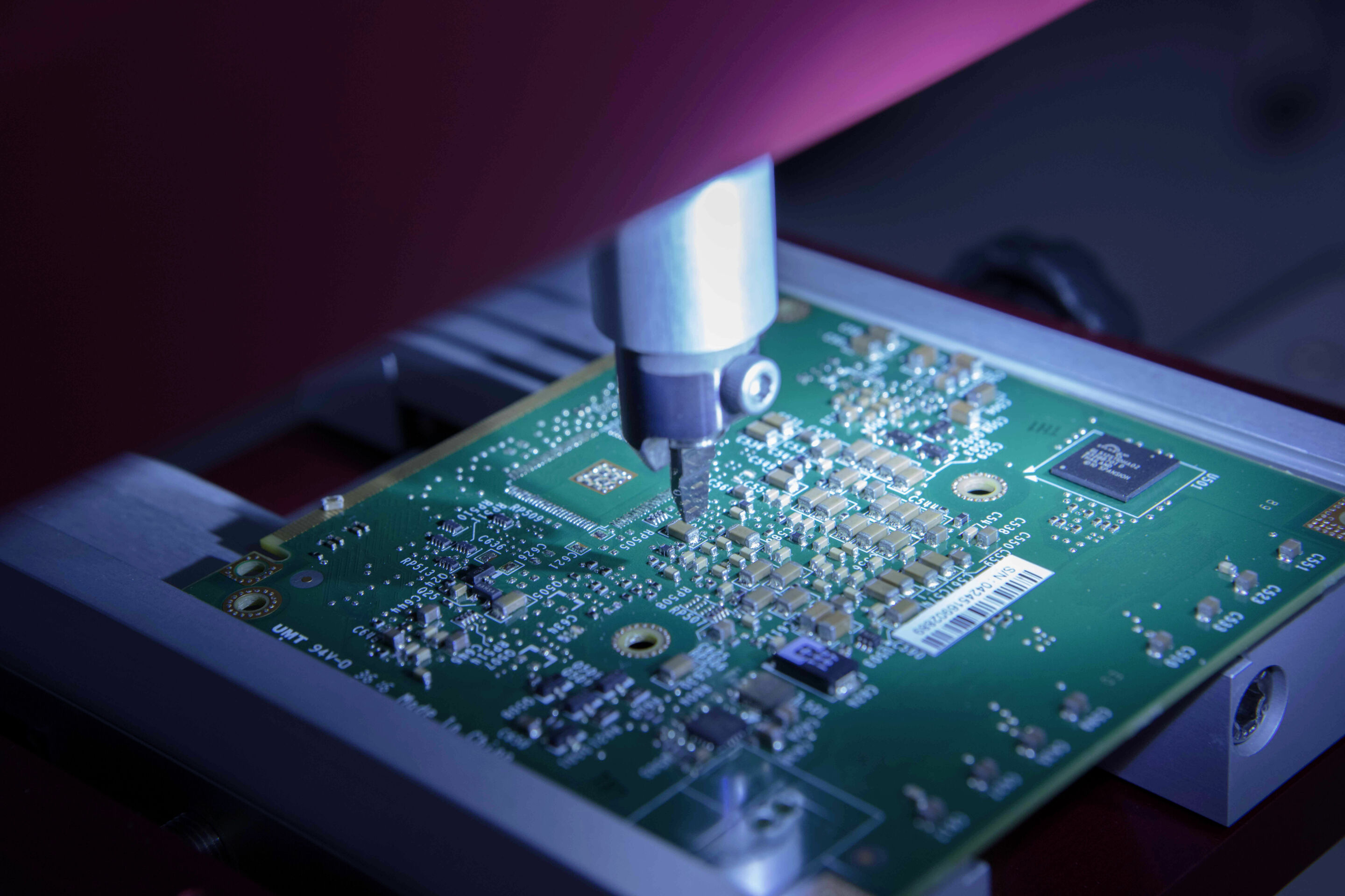
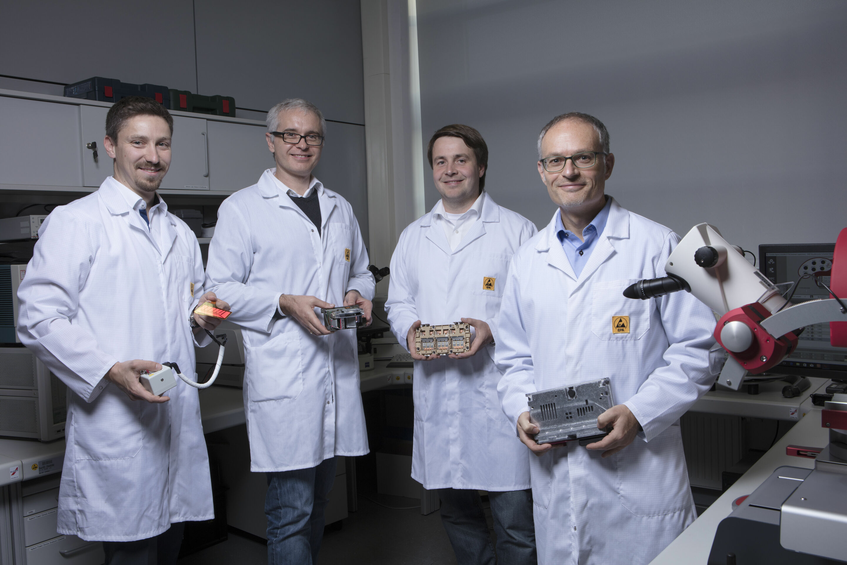
Automated driving, powertrain electrification, and the increasing networking of cars with one other and their surroundings – all these innovations are based on powerful semiconductor technologies. “More than 80 percent of all innovations in today’s automobiles are made possible by microelectronics,” said Stefan Simon, semiconductor expert at Quality Assurance. “All told, a car today includes as many as 8,000 active semiconductors in up to 100 interconnected control units. Every single one of them has more computing power than the first moon rocket.”
The Audi Semiconductor Lab works according to the principle of preventive quality management. As a central point of contact for the topics of semiconductor quality and analysis as well as assembly and connection technology, it fulfills an important interface function. This applies both within the company and in contact with external partners from industry and research.
As a competence center, the Semiconductor Lab supports the cross-business and interdisciplinary assessment of components and assemblies as well as manufacturing and production processes. Another core task is the qualification of employees in all specialist areas. This spectrum of topics makes Audi’s Semiconductor Lab unique in the European automobile industry.
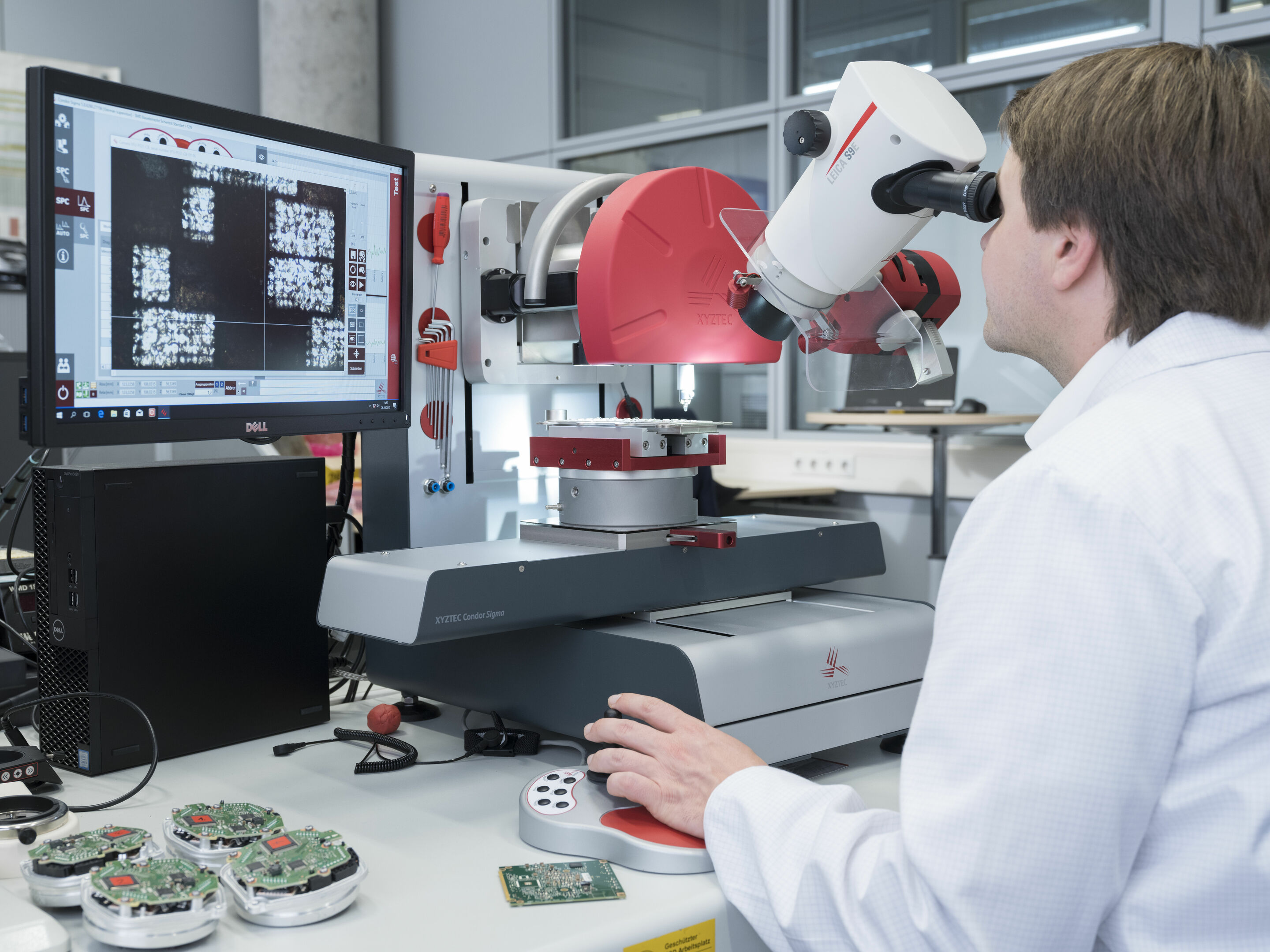
The experts at the Semiconductor Lab assess the individual components – the inner workings of the control units – for suitability, reliability and production quality. Early in the development process, staff check the requirements that a semiconductor chip has to meet for use in automobiles. And these clearly differ from those for other applications. While the average life of a smartphone is two years, it is about 15 years for a car. What’s more, the use and strains to which a car is subjected cannot be compared to those of a smartphone. “A semiconductor has to be designed and manufactured differently to account for the temperature differences, moisture and vibrations that occur in an automobile,” explained semiconductor expert Oliver Senftleben.
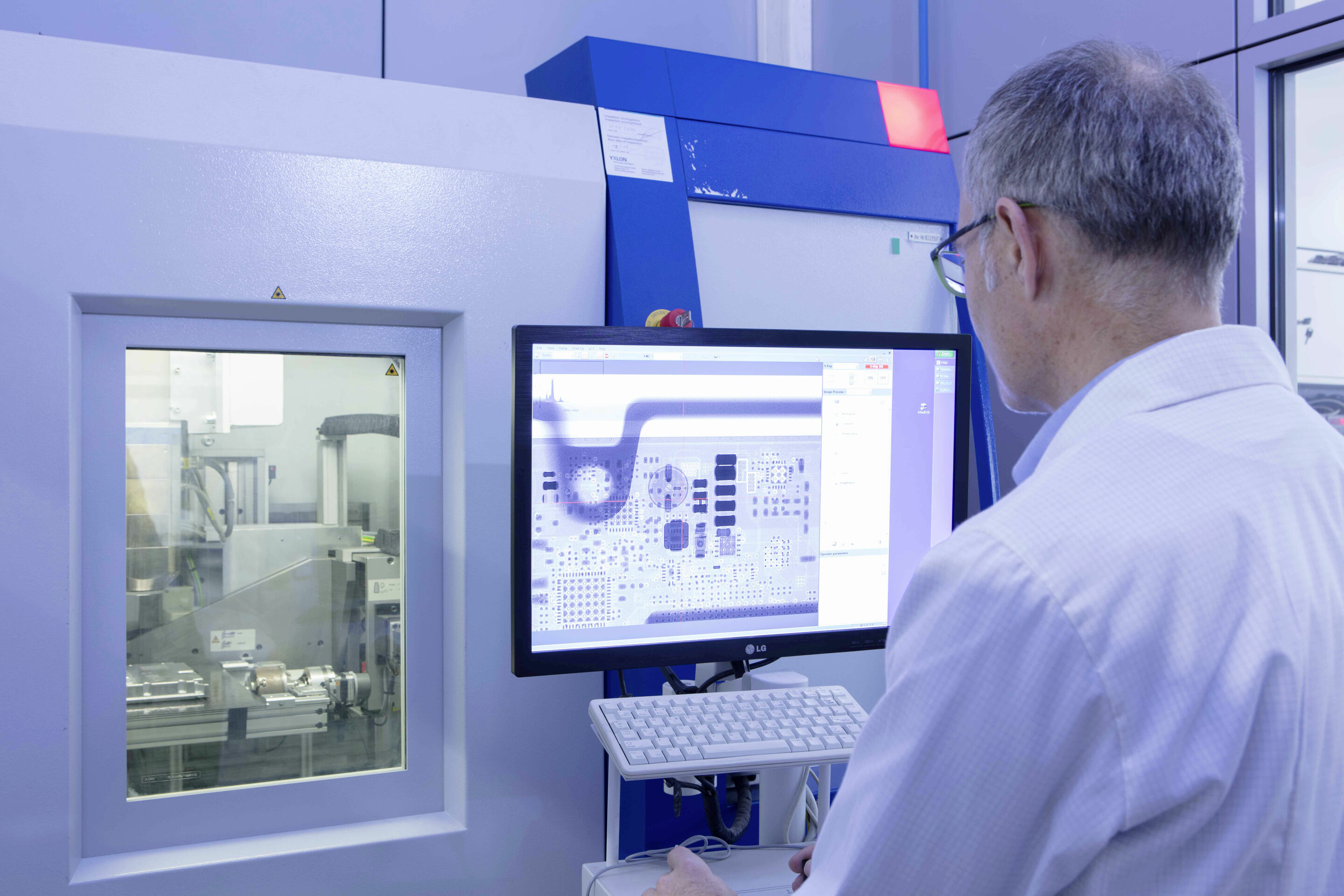
Components can be tested in the lab for aging mechanisms as they can occur in the car. Aging in a climate chamber is one such a test. Physical analyses are also used to investigate aging behavior and production qualities. Among other things, the Semiconductor Lab is equipped with a modern x-ray machine and a scanning electron microscope. For special analyses of semiconductor chips, the experts work closely with the colleagues of the Lab for Materials Engineering, e.g. on sample preparation using the focused ion beam (FIB), a scanning electron microscope with a focused ion beam. This can be used to examine control units for possible series and process errors.
Digitization
Priorities have changed dramatically in recent years. Although drivers continue to compare the performance of vehicles whilst also keeping a close eye on design aspects, they also expect new technologies such as live traffic data via Audi connect, as well as problem-free connection of their smartphone with the vehicles and the latest driver assistance systems.
To meet these customer requirements, the automotive industry must increasingly turn to new, trendsetting technologies. Previously, components were only deemed suitable for use in the automotive industry after several years of use in consumer electronics. Nowadays, such components rapidly make their appearance in vehicles. To ensure that the electronics deliver the desired high performance, they are validated in advance. To safeguard Audi’s high quality standards, the Semiconductor Lab performs such tasks as the definition of requirements and a technology assessment. Standards that are customary in the consumer sector (0 °C to 40 °C) are compared with the standards of the automotive industry (-40 °C to 125 °C) and lifetime requirements are checked. For example, the Audi MMI connect app can be used to query the current status of the vehicle, operate the interior climate control system or check the charge status. The car is thus constantly connected to and in communication with the environment, resulting in significantly increased uptime of the connected components. These can be active for as many as 30,000 hours and more in a vehicle life cycle. And some future applications will have to be equipped as “always-on” solutions.
autoSWIFT – tailored electronic components for the automobile industry
In order to come up to the high innovation tempo in the industry and to be able to rapidly react to new developments, AUDI AG collaborates with leading partners in the semiconductor segment and the electronics industry. Together with FZI Forschungszentrum Informatik, Globalfoundries, HOOD GmbH, Infineon Technologies AG and Robert Bosch GmbH, the fundamentals for a standardized technology assessment will be established. The “autoSWIFT” research project stands for “rapid innovation cycles for electronics systems throughout the automobile added value creation chain”. It has set its sights on getting innovative and high-quality electronics components based on the latest manufacturing technologies much quicker and in a much more appropriate way than before into vehicles. For future requirements placed on this development process, it is currently being investigated how the value creation chain can be turned into a value creation network.
“The cross-company and interdisciplinary joint development of automotive components is intended to enable the suitability of future technologies to be assessed during their development phase and incorporated into the product development processes sooner than before,” explains Helmut Lochner, expert from the Semiconductor Lab and autoSWIFT overall project leader. This will bring the latest semiconductor technologies into harmony with the high quality standards of the automotive industry.
Lighting technology
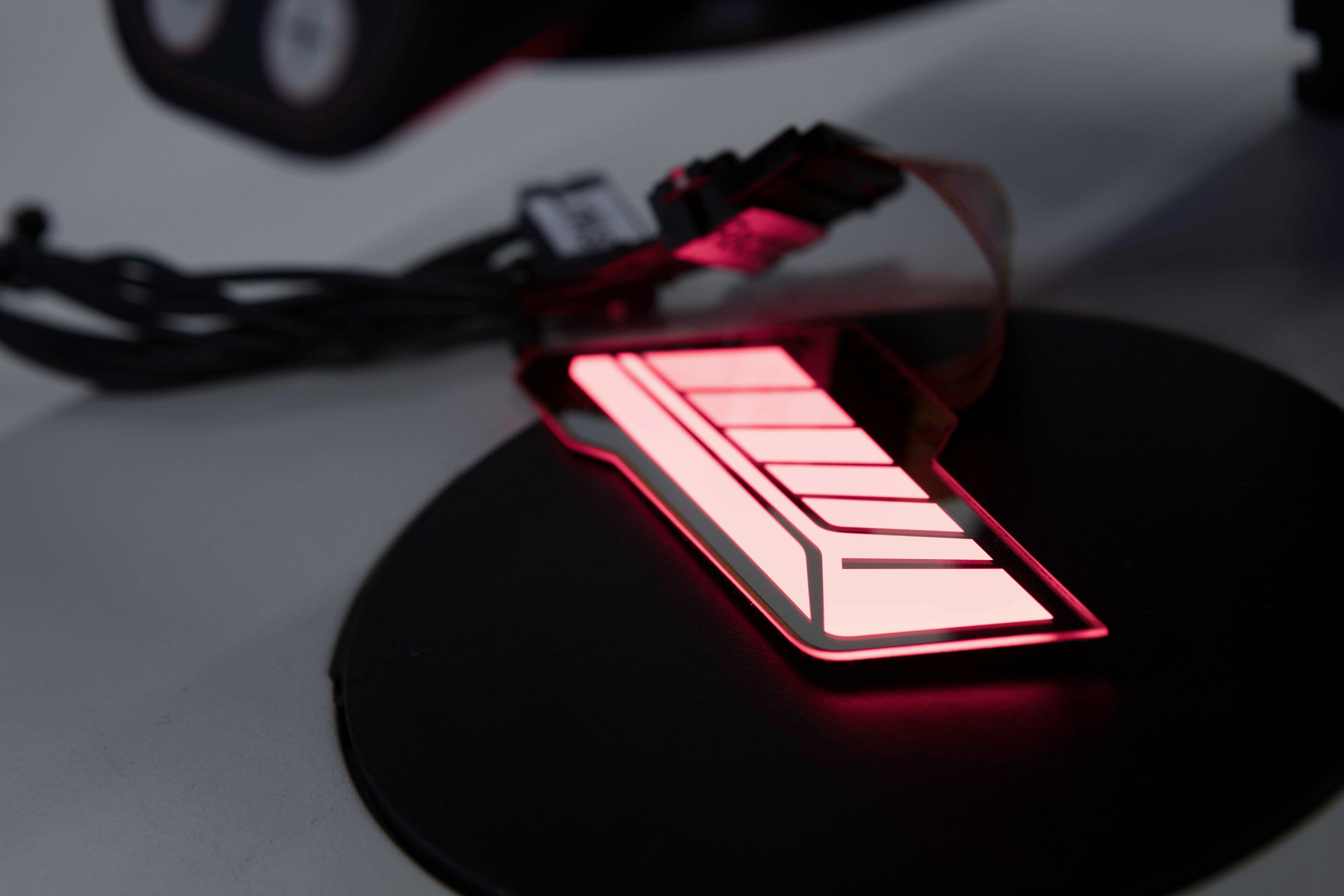
For the new Audi A8 and the Audi TT RS (combined fuel consumption in l/100 km: 8.5 - 8.2*; combined CO2 emissions in g/km: 194 - 187*), the brand with the four rings optionally offers tail lights with OLED technology (OLED: Organic Light Emitting Diode). Unlike single-point light sources, such as LEDs, OLEDs are so-called surface light sources. Their light takes homogeneity to a new level. They do not cast any harsh shadows and require no reflectors, light guides or similar optical parts. This makes the OLED units efficient and light – with minimal space requirements. The division of the OLEDs into small, individually controllable segments with a three-dimensional arrangement enables completely new lighting scenarios, which give the designers additional creative freedom in design and animation.
In each OLED unit, two electrodes – at least one of which is transparent – incorporate numerous extremely thin layers of organic semiconductor materials. A low voltage causes these layers, which are 200 times thinner than a human hair, to illuminate. This has allowed the traditional Audi genes to be transposed into a new technology.
The employees of the Semiconductor Lab were part of the multi-stage validation process to which this innovative lighting technology was subject prior to its series-production introduction. This ranged from the creation of specific implementation profiles to the validation of the basic technology and the OLED module, right up as far as the testing of the complete tail lights. The focus was on the unique aspects of use in the automotive sector, e.g. aging behavior due to environmental influences and passive aging.
The first-ever use of OLEDs in the automotive sector required the derivation and review of specific parameters of this technology. Audi’s Semiconductor Lab, in conjunction with Technical Development, carried out a complete technology assessment for each application during the pre-development phase. Weak points in the technology and in the manufacturing process were identified and addressed. These specific requirements for OLED technology have been defined for future projects and anchored as a standard.
Electrification
Audi is pressing ahead with the electrification of its drive systems across a broad front and is developing sustainable mobility concepts. As part of this, the power electronics form the beating heart of every electrified vehicle. Their core is formed by the pulse width modulating inverter – from a technological point of view, this is one of the most demanding components.
It converts the DC voltage from the high-voltage battery into three-phase alternating current for powering the electric motor. The high-performance semiconductors within the pulse width modulating inverter have a surface area of around 1 cm2 (0.4 sq in). Each of them must switch a current of more than 100 amps at a frequency of 10 kHz. Despite efficient cooling, the resultant in-chip power losses lead to rapid aging of the electrical contact connections.
Beginning with the Audi Q5 hybrid quattro (2011), then the Audi Q7 e-tron quattro (2016; combined fuel consumption in l/100 km: 1.9 - 1.8*; combined energy consumption in kWh/100 km: 19.0 - 18.1*; combined CO2 emissions in g/km: 50 - 48*) and the up-coming fully-electric Audi e-tron (2018), the employees of the Semiconductor Lab have supported and ensured the progression of the technological development in the power electronics. Examples of their work include evaluating the technological connections between the individual chips and the heat sinks, and subsequently ensuring the necessary thermal connections. In doing so, the aging mechanisms were focused upon just as much as the specificities of the process involved in the individual technologies. Among these were soldering, wire bonding and sintering – the so-called mounting and connection technologies. The results were of fundamental importance for the creation of a Group-wide norm, which was partially converted into a German industrial standard in 2017.
RoBE – Robustness for Bonds in E-Vehicles
To enable a reliable service life prognosis for each individual bond during production, Audi has teamed up with partners from industry and research in the joint RoBE (Robustness for Bonds in E-Vehicles) project. The goal is to at least double the bond life typical for consumer electronics. The project, which also includes the Fraunhofer IZM and Fraunhofer ILT research institutes, strives for a deeper understanding of the variables and the mechatronic relationships of bonding technology. Alternative production techniques such as laser beam welding are being developed and new wire materials investigated in order to overcome today’s process limits.
The most important lever for the collaborative research of innovative solutions by industry and research institutes is the pooling of competencies along the entire development and creation chain. Assessment criteria and test standards for novel technologies often do not yet exist. The Semiconductor Lab is therefore involved in the development of Group-specific quality specifications at very early project and pre-development stages, and even drives their development across industries.
Automated driving
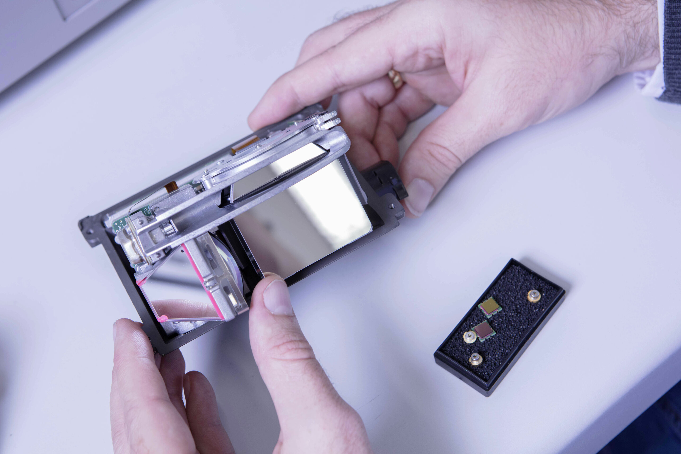
The new Audi A8 is the world’s first volume-production car to be designed for conditional automated driving at Level 3 in accordance with international standards. The Audi AI traffic jam pilot takes charge of driving in slow-moving traffic at up to 60 km/h (37.3 mph) on highways and multi-lane roads with a physical barrier dividing the opposing lanes. During piloted driving, a central driver assistance controller (zFAS) now permanently computes an image of the surroundings by merging the sensor data. In addition to the radar sensors, a front camera and the ultrasonic sensors, Audi is the first car manufacturer to also use a laser scanner.
The scanner expands the long-range radar’s field of view from a narrow 35 degrees to 145 degrees. Thanks to the wide coverage, the car will be able to identify other road users and interpret their behavior, such as moving into and out of the lane, much sooner in the future. “You can think of the laser scanner as a beam of light scanning the car’s surroundings in fractions of a second,” said Robert Kraus, an expert in production technologies at the Semiconductor Lab. A rapidly rotating mirror inside the compact housing guides the beam of the powerful laser diode in small increments across the area to be scanned. The new laser scanner doesn’t just detect obstacles, it can also determine the exact distance to them. It does this by measuring the time between the emission of a laser pulse to its detection at the photodiode.
The employees of the Semiconductor Lab have been preparing for the successful first use of the laser scanner in the new A8 since 2014. In collaboration with Technical Development, they defined comprehensive specifications and requirements of the part and its individual components. Before being used for the first time in the automotive branch and having previously only been used in consumer electronics, the laser diode was subject to numerous reliability tests and detailed analyses as part of complex laboratory trials. On the basis of these results, optimizations in the manufacturing process for diodes were brought about in order to fulfill the quality requirements needed of them.
* Figures depend on the tire/wheel set used and the number of seats
Subject to change without notice; errors and omissions excepted.